If you are searching about SEM cross section of the chip. | Download Scientific Diagram you've came to the right page. We have 20 Pictures about SEM cross section of the chip. | Download Scientific Diagram like Chip resistor corrosion - SEM Lab Inc., Resistor Failure Analysis - SEM Lab Inc. and also Resistor Failure Analysis - SEM Lab Inc.. Here it is:
SEM Cross Section Of The Chip. | Download Scientific Diagram
sem section
Resistor Failure Analysis - SEM Lab Inc.
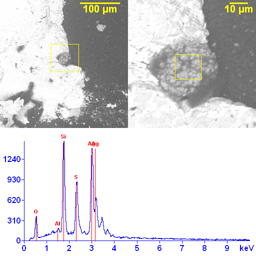 www.semlab.com
resistor corrosion apparent eds sulfide
Figure 1 From Corrosion Behavior Of Cu-Al Intermetallic Compounds In
 www.semanticscholar.org
intermetallic corrosion wire bonding behavior compounds accelerated containing chloride humidity
SEM Images Of Corrosion Features: (a) Bridging Of Anode And Cathode
 www.researchgate.net
SEM Photo Showing The Cross-section Of The Wafer After Dicing Through
 www.researchgate.net
wafer after dicing cmos mems tsv
SEM Images Of The Die Attached Sample At 390°C Represents: A) Bulk
 www.researchgate.net
Figure 1 From Comprehensive Study On Effect Of Chip Layout And Mold
 www.semanticscholar.org
SEM Of Severe Corrosion That Occurred At The Edge Of The Aluminum
 www.researchgate.net
thin batteries severe corrosion occurred
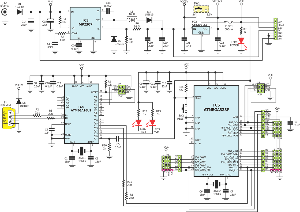
Edit Free Photo Of Circuits,electronics,atmel,atmega328,arduino
 www.needpix.com
Chip Resistor Corrosion - SEM Lab Inc.
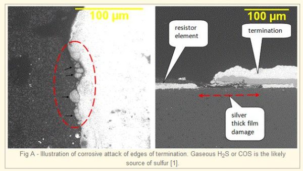 www.semlab.com
Study Of Chip–Package Interaction Parameters On Interlayer Dielectric
 www.semanticscholar.org
parameters interaction chip crack dielectric interlayer propagation
Figure 1 From Development Of Flip Chip Die Bump Temperature Measurement
 www.semanticscholar.org
Typical SEM Images Of Al–8Cu–3Si Alloy Showing: Corrosion Products At
 www.researchgate.net
corrosion 8cu 3si alloy
Layout Of The Proposed Circuit. The Die Area Is 106 μm × 146 μm
 www.researchgate.net
How To Avoid The Side Corrosion Process Of Pcb Circuit Processing – Artofit
 www.artofit.org
AI Emoji Generator
SEM Images Of The Chip Shapes And Underside Surfaces Produced By Coated
 www.researchgate.net
Figure 2 From Corrosion Of Copper Wire Bonded Packages By Chlorine
 www.semanticscholar.org
SEM Images Of The Core Chip. (a) Frontside. (b) Backside. | Download
 www.researchgate.net
Test-chip Die Photo: Transistor Structure, Track-and-latch Comparator
 www.researchgate.net
Typical sem images of al–8cu–3si alloy showing: corrosion products at. Layout of the proposed circuit. the die area is 106 μm × 146 μm. Figure 2 from corrosion of copper wire bonded packages by chlorine